|
Description:
|
|

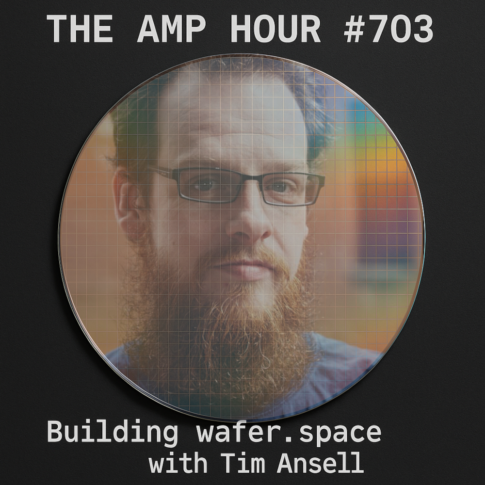
Welcome back Tim Ansell!
- Tim’s past appearances and previous work
- Tiny Tapeout
- Matt Venn’s Tiny Tapeout program further subdivides the manufacturing costs, making it the cheapest way to create custom silicon, typically costing around $300 per design.
- Tiny Tapeout lowers the barrier to entry, allowing people to “just try it and see if you like it,” similar to writing a “hello world” program.
- The program has already processed almost 3,000 projects, demonstrating high community demand when costs are low.
- Despite limitations, advanced projects are possible: a developer taped out a Linux capable SOC using open-source tools and the tiny tapeout space.
- Introducing Wafer Space
- Tim started Wafer Space, based in Singapore, to provide community access to open-source manufacturing after EFABless ceased operations.
- Wafer Space focuses on the GF-180 MCU PDK (Global Foundries 180 nm process), which is a much cheaper technology manufactured in Singapore.
- The core offering is a low-volume production run: $7,000 USD gets you 1,000 chips back. This volume is enough for prototyping and shipping a small product (e.g., 500 units).
- The design envelope area is 3.8 x 5 mm (20 mm squared) using the 180 nm process.
- Interested parties should sign up via the Crowd Supply page. The current target timeline is submissions by December 3rd, with delivery by March 15th.
- Manufacturing & Packaging
- By default, customers receive bare silicon die
- Tim is working with PCB manufacturers (like JLC PCB, PCB Way, Seed Studio) to offer Chip on Board (COB) wire bonding assembly onto custom PCBs (think black epoxy blob on a PCB)
- COB packaging is significantly cheaper (sub-$2) than standard packaging houses (which often charge around $7 per chip).
- This approach also provides faster iteration speed, as PCB manufacturers offer quick turnaround times (sometimes 3 days) compared to typical packaging houses (3 months)
- Getting Started & Resources
- If you are new to chip design, starting with Tiny Tape Out’s click and drag tools is highly recommended. Matt Venn previously talked/sang about Siliwiz
- More advanced tools include Verilog and VHDL (coding style) or KLayout and Magic (drawing shapes, similar to PCB design).
- To follow the project or seek help, join the Wafer Space Discord
- New services offering open-source silicon manufacturing include IHP (Europe/130 nm) and Chip Foundry (US/Skywater), increasing ecosystem resiliency.
- Website: Wafer.space
- Sign up on the CrowdSupply campaign
|
 More
More
 Religion & Spirituality
 Education
 Arts and Design
 Health
 Fashion & Beauty
 Government & Organizations
 Kids & family
 Music
Music News & Politics
 Science & Medicine
 Society & Culture
 Sports & Recreation
 TV & Film
 Technology
 Philosophy
 Storytelling
 Horror and Paranomal
 True Crime
 Leisure
 Travel
 Fiction
 Crypto
 Marketing
 History

.png)
 Comedy
 Arts
Arts Games & Hobbies
 Business
 Motivation